


Mega-chipping Eindhoven
Philips’ participation in the European mega-chip project ended with a drastic reorganization that reshaped its home base of Eindhoven and opened the doors for new high-tech companies such as ASML.
Via incentive programs, Europe tried to catch up with information-technology front-runners in America and Asia. In 1984, Philips and the German company Siemens joined the European Union program for the development of information technology (ESPRIT). Together they had approximately one billion Euros to spend.
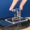
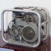
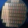
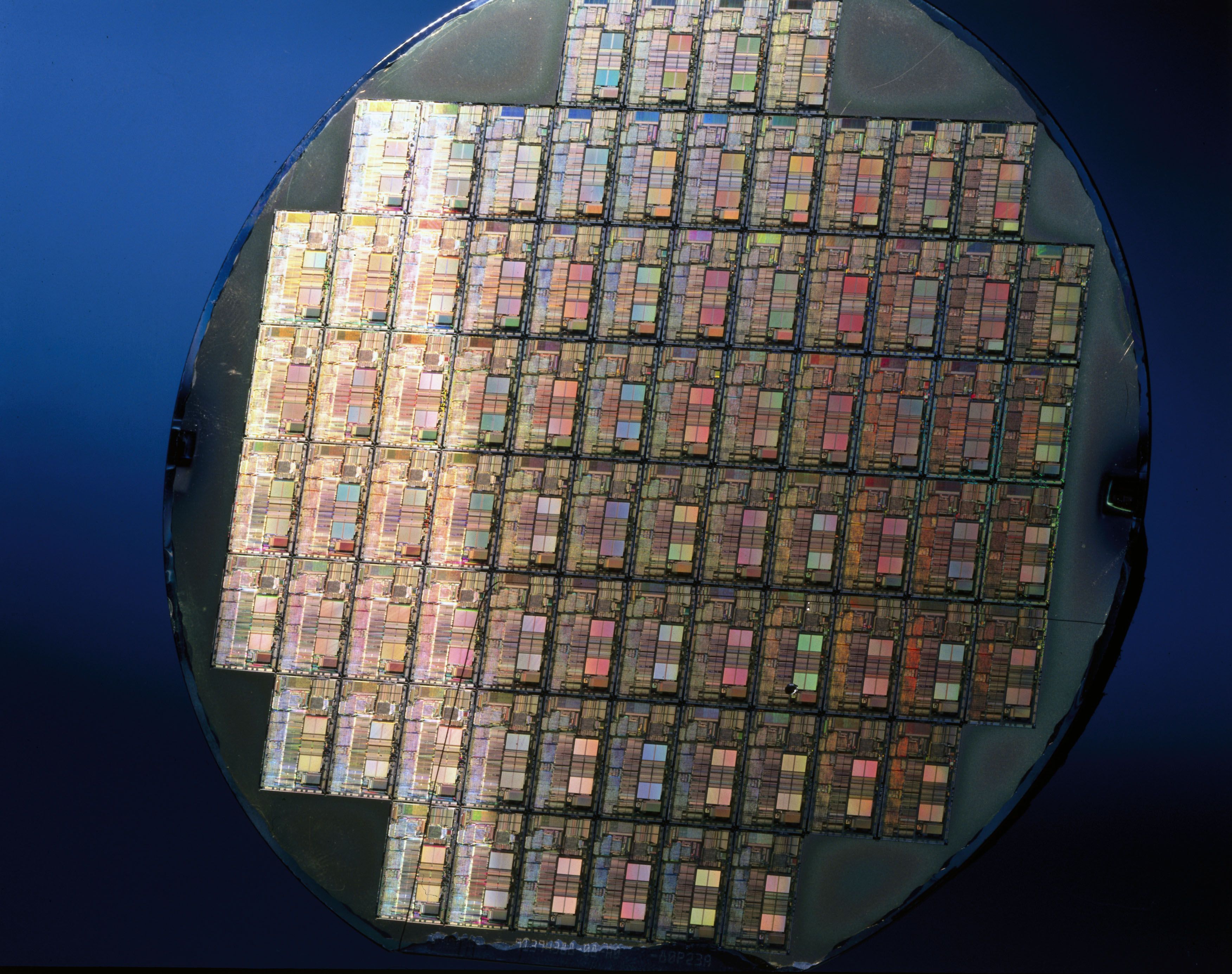
In Eindhoven, Philips moved into the development of permanent memory chips. Next door to the NatLab, it created labs with clean rooms, and in a joint venture with ASM-Lithography (ASML) from Veldhoven, it produced wafer steppers by its own design. Within three years, Philips was Europe’s largest chip producer and the seventh largest in the world.
However, profits were disappointing, as were the returns on consumer electronics. Philips centennial party in 1990 was overshadowed by the upcoming ‘Operation Centurion’ reorganization (1990–1997) that was necessary to rescue the company. On a global scale, 50,000 jobs disappeared. Company departments closed or were hived off.
The impact on Eindhoven was immense and the city was forced to request support from European restructuring funds. Start-ups and spin-offs based on Philips activities, like the privatized ASML, gave new structure to the region. Collaboration between organizations in the fields of research and education were at the heart of these initiatives.
The High-Tech Campus that appeared around the buildings of Philips Research became the symbol of Brainport Eindhoven, the world’s smartest region.
How to cite this page
Frank Veraart, 'Mega-chipping Eindhoven', Inventing Europe, http://www.inventingeurope.eu/story/mega-chipping-eindhoven
Sources
- Michel Carpentier, ‘ ESPRIT, Prestaties en Hoop’ in Teye Buma, Wetenschap en technologie in Europa, onderzoek en ontwikkeling in 20 landen, Foundation Scientific Europe, Maastricht, 1990, p. 288-297
- Ina Horlings, Afstand en betrokkenheid, Perspectieven op duurzame gebiedsontwikkeling, Telos, Tilburg, 2009
- Irene Lammers, Pim Eling, Ard-Pieter de Man and Arjan van Weele, ´Meeting Moore’s Law: High Velocity Knowledge Development in the Supplier Network of ASML´ in Ard-Pieter de Man (ed.) Knowledge Management and Innovation in Networks, Edward Elgar, Cheltenham, 2008
- Marcel Metze, Kortsluiting. Hoe Philips zijn talenten verspilde, SUN Nijmegen, 1991
- Website ASML http://www.asml.com (History)